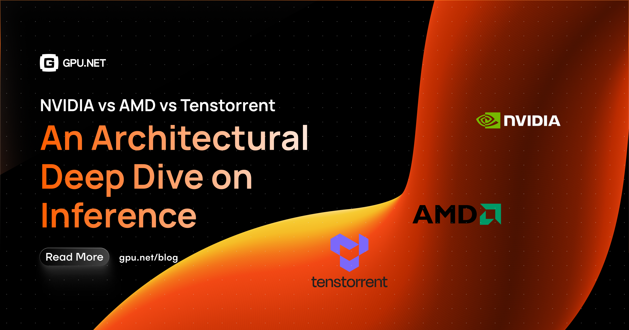
NVIDIA vs AMD vs Tenstorrent: An Architectural Deep Dive on Inference
This piece tries to do the most: line up NVIDIA, AMD, and Tenstorrent side by side at the architectural level - execution model, memory hierarchy, interconnect, software stack, and the strategic shape of each company's bet - and explain why Tenstorrent's choices, while less proven, are particularly well-fitted to the direction inference workloads are heading. The question is not 'which is best today' but 'which architectural lineage is best matched to where inference is going, and why does that matter for buyers and operators?' This is Part 5 of the AI Inference Hardware series.
Introduction
This piece is the longest in the series because it tries to do the most: line up NVIDIA, AMD, and Tenstorrent side by side at the architectural level - execution model, memory hierarchy, interconnect, software stack, and strategic shape - and explain why Tenstorrent's choices, while less proven, are particularly well-fitted to where inference is heading.
As of mid-2026, NVIDIA still wins most inference workloads on raw deployability, ecosystem maturity, and predictable performance. The question this article is asking is not "which is best today" but "which architectural lineage is best matched to where inference is going, and why does that matter for buyers and operators?"
Execution Model: SIMT, SIMD-Heavy MIMD, or Mesh MIMD
The single most consequential architectural difference between the three companies is how they organize parallel execution.
1. NVIDIA Hopper and Blackwell - SIMT
- Single Instruction, Multiple Thread execution.
- A streaming multiprocessor schedules warps of 32 threads that execute in lock-step.
- Hardware manages divergent branches via per-thread masks.
- Warp scheduling hides memory latency by switching active warps when one stalls on DRAM.
- H100: 132 SMs, fourth-generation Tensor Cores, FP8 Transformer Engine, ~256 KB shared memory / L1 cache per SM.
- B200: Doubles the chiplet count (two dies in one package), adds fifth-generation Tensor Cores with native FP4 support.
Strengths:
- Extraordinarily well-suited to dense, batched matrix multiplication on regular tensors.
- Latency-hiding through warp scheduling means programmers don't have to think carefully about every memory access.
- CUDA toolchain abstracts the parallelism so kernels can run across GPU generations.
Weaknesses:
- Wasteful for irregular workloads. When threads in a warp diverge (e.g., MoE expert routing), some lanes idle while others compute.
- Latency hiding works less well for irregular memory access patterns.
- The abstraction tax means programmers cannot easily get below CUDA to optimize specific data movement patterns.
2. AMD CDNA 3 and CDNA 4 - SIMT (wider warps)
- Same SIMT model with 64-thread warps (vs NVIDIA's 32).
- MI300X: 304 compute units across multiple chiplets.
- MI355X: Fully featured FP4 and FP6 support in CDNA 4.
Chiplet design:
- 3D packaging: Accelerator Compute Dies (XCDs) fused with I/O Dies (IODs) using 3D stacking.
- 2.5D packaging: IODs connected to each other and to twelve HBM3E stacks.
Memory bandwidth and capacity are the standout figures:
- MI300X: 192 GB HBM3 @ 5.3 TB/s
- MI325X: 256 GB HBM3E @ 6 TB/s
- MI355X: 288 GB HBM3E @ 8 TB/s
Strengths: Very similar to NVIDIA - outstanding throughput on dense matrix workloads, mature kernel libraries.
Weaknesses: Software ecosystem (ROCm) is meaningfully behind CUDA in tooling depth, kernel optimization breadth, and the precise tuning that delivers the last 20% of advertised performance.
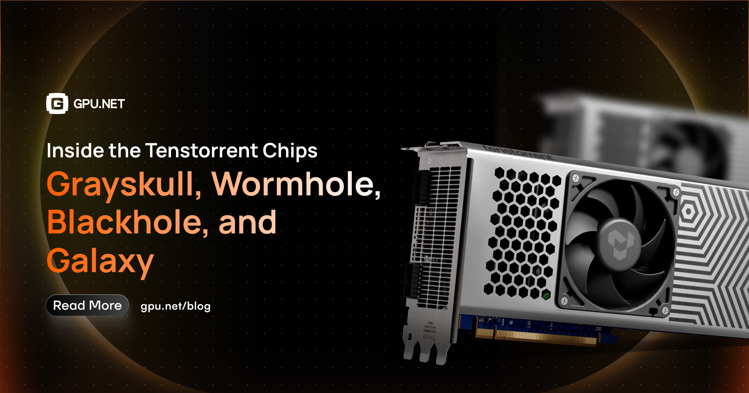
3. Tenstorrent Wormhole and Blackhole - Mesh MIMD
A clean architectural departure:
- No SIMT. Each Tensix core is a MIMD compute tile with its own instruction stream.
- Inside a Tensix core: five small RISC-V "baby" cores coordinate matrix and vector engines plus pack/unpack units, with 1.5 MB of local SRAM.
- Across a chip: Tensix cores arranged in a 2D mesh connected by a network-on-chip.
- Across chips: mesh extends via 400 Gbps Ethernet (Wormhole) or 800G QSFP-DD (Blackhole) - no PCIe switches, no proprietary fabric.
The radical part:
- No cache hierarchy. Data lives in DRAM, in another core's SRAM, or in this core's SRAM - software moves it explicitly via DMA.
- Memory access is deterministic - every DRAM read takes a known number of cycles.
- No hardware multithreading. Tensix cores operate via cooperative processing, with explicit software pipelining replacing warp-based latency hiding.
Why this matters for inference:
- Transformer inference has a very specific data flow pattern: load weights once, stream activations through layer by layer, write KV-cache back.
- Data movement pattern is highly structured.
- SIMT's flexibility is wasted; deterministic explicit data movement is exactly the right primitive.
- Mesh topology means scaling out doesn't require an expensive switch hierarchy.
- Absence of caches means the compiler can schedule data placement perfectly - no eviction surprises.
Trade-off: Programmability. Writing a Tenstorrent kernel in TT-Metalium is genuinely harder than writing a CUDA kernel - you have to think about which SRAM lives where, when data flows across the NoC, and how to overlap compute with movement.
Memory Hierarchy: Where the Inference Money Is Made or Lost
Inference is bottlenecked far more often by memory than by compute. The KV-cache for long-context inference can be larger than the model weights themselves.
NVIDIA
- H100 SXM: 80 GB HBM3 @ 3.35 TB/s
- H200: 141 GB HBM3e @ 4.8 TB/s
- B200: up to 192 GB HBM3e at higher bandwidth
- Bandwidth gains drive performance: H200's 1.83-2.14x inference speedup over H100 on long-context Llama-class workloads comes from HBM3e.
- H100 drops 64% of throughput as context scales; H200 holds up better (47% drop).
AMD
- AMD has positioned memory as its primary lever:
- MI300X: 192 GB HBM3 @ 5.3 TB/s
- MI325X: 256 GB HBM3E @ 6 TB/s
- MI350 series: 288 GB HBM3E @ 8 TB/s
- Largest single-chip memory pools in production AI hardware today.
- Why MI300X became the de facto choice for memory-bound inference despite the ROCm gap.
Tenstorrent
- Wormhole: 12 GB GDDR6 per chip @ 288 GB/s.
- Blackhole: 28-32 GB GDDR6 per chip @ ~1 TB/s estimated.
- Dramatically behind both NVIDIA and AMD on per-chip memory capacity and bandwidth.
Strategic answer - distributed on-chip SRAM and mesh-scaled DRAM pooling:
- Each Blackhole chip carries 180-210 MB of SRAM distributed across the Tensix mesh.
- Across a Galaxy of 32 Blackhole chips, that aggregates to 6.2 GB of on-chip SRAM at 2.9 PB/s - orders of magnitude faster than any DRAM.
- Total DRAM in a Galaxy: 1 TB at 16 TB/s aggregate, accessed through the on-chip Ethernet mesh and treated logically as a unified memory pool.
The cost angle:
- GDDR6 is much cheaper than HBM3/HBM3e - hundreds of dollars per chip difference.
- Tenstorrent's bet: aggressive use of distributed SRAM plus mesh DRAM pooling delivers competitive or better effective bandwidth at substantially lower cost per chip.
- Savings compound at rack and supercluster scale.
Interconnect: The Part Most People Underestimate
Interconnect is where data center economics live or die.
NVIDIA
- NVLink 4.0 at 900 GB/s bidirectional aggregate per GPU within HGX/DGX.
- NVSwitch for all-to-all communication.
- InfiniBand or RoCE for multi-node networking.
- Fast, expensive, proprietary.
- NVSwitch hardware and associated licensing add meaningful cost.
- GB200 NVL72: 72 Blackwell GPUs in one rack tied together by fifth-gen NVLink at 1.8 TB/s per GPU.
AMD
- Infinity Fabric serves a similar role inside 8-way MI300X servers.
- Faster generationally with MI355X but still proprietary.
Tenstorrent
- Integrated 400 Gbps Ethernet directly onto each Wormhole chip.
- 800 Gbps Ethernet onto each Blackhole chip.
- Scaling out = passive QSFP-DD cable from one chip to another. No NVSwitch, no InfiniBand switches, no proprietary fabric.
- On-chip 2D mesh and off-chip Ethernet form one continuous logical network.
- Exposed to software as one big mesh of Tensix cores.
Specific consequence at scale:
- Tenstorrent Galaxy: 32 Blackhole chips on a single board with 56 x 800G Ethernet ports (11.2 TB/s).
- 4 Galaxies form a "quad."
- Quads connect into superclusters via cabled all-to-all topology - idle quads repurposable as switches.
- Tenstorrent on record: "Critically, there are no Ethernet switches anywhere in the design."
Tenstorrent's TT-Fabric specification claims a 10x TCO advantage for AI data center design from this approach. Number is from Tenstorrent's own modeling - the structural argument (no switch tax, no proprietary fabric tax) is sound regardless.
Software Stack
1. NVIDIA
- CUDA at the bottom
- cuDNN, cuBLAS for linear algebra
- TensorRT-LLM for optimized inference
- Triton Inference Server for serving
- NIM containers for one-click deployment of pre-optimized models
- Rich third-party ecosystem (vLLM, SGLang, TGI, Ollama) targets CUDA first
Depth of optimization at every layer is unmatched. Cost: total vendor lock-in.
2. AMD
- ROCm
- HIP (CUDA-like C++ extension) at lower level, with translation layers
- MIOpen for linear algebra
- Compatibility with PyTorch, vLLM, SGLang is solid
- Meta production partnership has driven significant maturity
- Open-source in name and increasingly in practice
3. Tenstorrent
Fully open-source Apache 2.0 across every layer:
- TT-Metalium - Bare-metal SDK, OpenCL-like C++ interface, direct access to RISC-V cores, NoC, matrix and vector engines.
- TT-NN - Operator library with a PyTorch-like Python API.
- TT-Forge - MLIR-based compiler bridging PyTorch, JAX, ONNX to hardware. Claimed support for 800+ model variants in CI.
- TT-LLK - Low-level kernel layer.
Maturity ranking: NVIDIA gold standard → AMD production-viable for common patterns → Tenstorrent rapidly improving but earliest in out-of-the-box experience.
Strategic Shape: Where Each Company Is Betting
NVIDIA
Betting that the GPU paradigm has decades more headroom, that CUDA's compounding ecosystem advantage is unassailable, and that vertical integration (chips + DGX systems + InfiniBand + NIM + software) will keep enterprise customers locked in.
Rubin roadmap (CES 2026) doubles down on unified compute, memory, and networking for long-context reasoning workloads.
AMD
Betting that being a credible second source - better memory, cheaper hardware, increasingly open software - is enough to take meaningful share from NVIDIA, especially in memory-bound inference.
MI400 roadmap, Helios rack-scale platform, and the Meta partnership all point in this direction.
Tenstorrent
Betting on architectural divergence. Not "better GPUs" but "the post-GPU architecture for AI": mesh-based MIMD, open RISC-V, open software, no switch hierarchy, distributed SRAM, scale-out by Ethernet.
The bet: inference workloads are becoming more diverse, more data-movement-dominated, and more sensitive to total cost of ownership - and a clean-sheet architecture purpose-built for those properties beats incremental improvements on a paradigm originally designed for graphics.
Why This Matters for Inference Specifically
The argument for Tenstorrent on inference is concrete:
1. Mixture-of-Experts Models
- Route different tokens to different experts.
- On a SIMT GPU, this causes warp divergence and underutilization.
- On a MIMD mesh, each core can independently run its assigned expert without lock-step coordination.
- DeepSeek V4-class models map naturally onto Tenstorrent's architecture.
2. Long-Context Inference
- Bottlenecked by KV-cache memory traffic.
- Tenstorrent's distributed SRAM acts as a fast scratchpad close to compute, reducing DRAM traffic.
- On-chip mesh allows KV-cache to be spread across many chips' SRAM rather than centralized in HBM.
3. Agentic Workloads
- Branching prompts, speculative decoding, varying batch composition.
- Benefit from the predictable latency of cache-free, software-scheduled memory access.
- SGLang and similar engines target exactly this pattern.
4. Cost Per Token at Scale
- GDDR6 (not HBM) + no switch fabric (Ethernet) + open-source software (no licensing) drives BOM costs lower per FLOP than equivalent NVIDIA or AMD systems.
- At rack and supercluster scale, this compounds.
5. Sovereign Deployment
- Procurement criterion, not technical one - but favors open hardware + open ISA + open software.
- Tenstorrent is the only player at meaningful scale that hits all three.
The Honest Counterpoint
None of this means Tenstorrent wins automatically:
- The software stack maturity gap is real.
- The per-chip memory disadvantage is real.
- The benchmark coverage compared to NVIDIA is sparse.
What it means is the architectural choices are well-fitted to where inference workloads are heading - and as workloads diverge from the dense-matrix-multiply pattern GPUs were designed for, Tenstorrent's bet becomes increasingly defensible.
Coming Next
In Part 6 - the final piece in this series - we look at proof-of-concept deployments, named companies actively using Tenstorrent, and what the published cost and performance numbers say about the real-world impact for buyers.
Sources: NVIDIA H100, H200, B200 product briefs; AMD Instinct MI300X, MI325X, MI355X technical disclosures; Tenstorrent docs.tenstorrent.com, tt-metal and tt-forge GitHub repositories, TT-Fabric architecture documentation; SemiAnalysis Blackwell TCO analysis; Spheron and GMI Cloud inference benchmarks; "HetGPU" (arXiv 2506.15993); Moor Insights & Strategy Tenstorrent analyst note; ASPLOS 2025 Blackhole microbenchmarking paper.


![GPUNET Verifiable Exchange: The Next Frontier for $GPU, Nodes and Ecosystem [TEASER]](https://i.ibb.co/Z1JWjN7r/Article-Cover.png)